APA102 LED CHIP
General Description
APA102 is a type ic for the three-color RGB Diming control strip and string ,This ic using the CMOS process
to provide three-color RGB LED output driver to adjust the output with 256 gray scale and 32 brightness adjustment
,APA with 2 signal output way , one is clock ,another is data, the clock and data is synchronizated ,so that the
crystal cascade piece of output movement is sychronizated .
Feature
CMOS process,low voltage ,low consumption
Synchronization of two-lane
Choose positive output or negative RGB three-color LED output
8 bit(256 level) color set ,5bit(32 level) brightness adjustment
Build-20ma constant current output
With self-detection signal build in support for continuous oscillation PWM
output ,can be maintained static screen
Application
LED lamp
LED Strip ,led pixel module
LED billboard LED screen
PRODUCT SPECIFICATIONS
|
Color
|
wavelength
|
Refresh rate
|
Voltage
|
Power
Consumption
|
Weight
(g)
|
Angle
|
Dimensions
(mm)
L*W*H
|
Operating
Temperature
|
|
Full color 1677216
|
R:500-650mcd
G:370-530mcd
B:120-165mcd
|
400 cycle
|
DC5V
|
0.2W
(MAX:1W)
|
1
|
160
|
5x5x1.4
|
-40-70℃
|
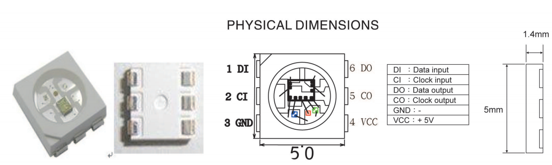
PIN Description)
|
NO.
|
PIN NAME
|
I/O
|
FUNCTION
|
|
1
|
VDD
|
P
|
Power is terminal
|
|
2
|
VREG
|
O
|
4.5V regulator output
|
|
3
|
CKO
|
O
|
Series with the output clock signal
|
|
4
|
SDO
|
O
|
Series with the output data
|
|
5
|
VEN
|
I
|
Self-test function selection
|
|
6
|
CSEL
|
I
|
Invert the clock signal cascade
|
|
7
|
POLAR
|
I
|
Positive and negative output options
|
|
8
|
OSCI
|
I
|
Oscillator input
|
|
9
|
SDI
|
I
|
Series with the input data
|
|
10
|
CKI
|
I
|
Series with the input clock signal
|
|
11
|
REXT
|
I
|
Constant current source to adjust side
|
|
12
|
VSS
|
P
|
Power supply negative terminal
|
|
13
|
G
|
O
|
Green LED output
|
|
14
|
R
|
O
|
Red LED output
|
|
15
|
B
|
O
|
Blue LED output
|
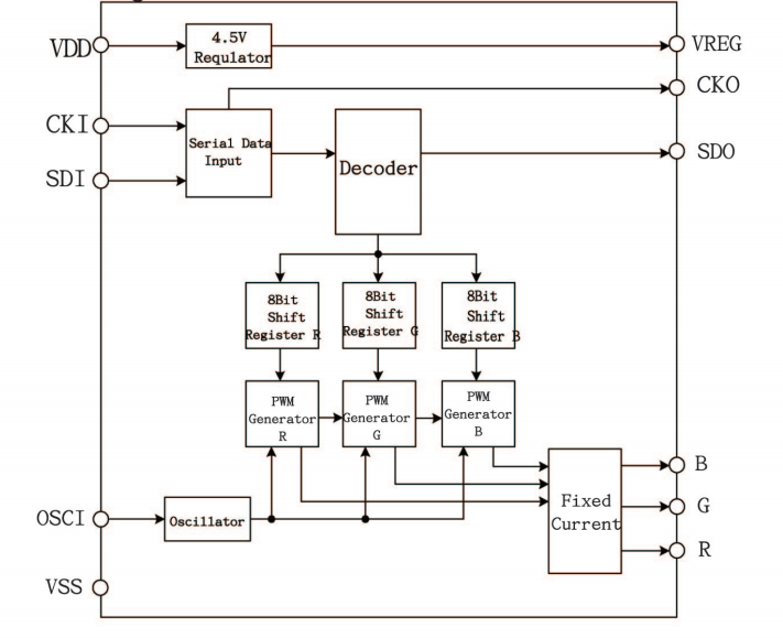
(Block diagram)
(Absolute Maximum Rating)
Supply volage -------------- -0.3-6.0V
Input voltage---------------- VSS-0.3 to VDD +0.3V
Operating temperature---------------- -40 to +70℃
Storage temperature------------------- -50 to +125℃
Note: Stress above those listed may cause permanent damage to the devices
(Electrical Characteristic)
|
Symbol
|
Parameter
|
Condition
|
Min.
|
Typ.
|
MAX
|
Units
|
|
VDD
|
Supply Voltage
|
|
|
5.0
|
5.5
|
V
|
|
VIH
|
Input High Voltage
|
|
0.7VDD
|
|
VDD+0.3
|
V
|
|
VH
|
Input Low Voltage
|
|
VSS-0.3
|
|
0.3VDD
|
V
|
|
LOL
|
Sink Current Voltage(RGB)
|
VDD=5V,VOL>1V
|
22.5
|
24.5
|
26.5
|
mA
|
|
RIN
|
Pull High
|
VDD=5V
|
|
570
|
|
kΩ
|
|
VREG
|
Regulator Voltage(VREG)
|
VDD=5V
|
4.4
|
4.5
|
4.7
|
V
|
|
FOSC
|
Oscillator Frequency
|
|
800
|
|
1200
|
KHz
|
(Function Description)
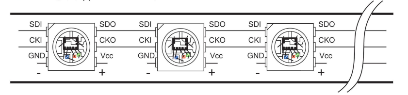
(1) cascading data structure
Tabdem N-LED

Global bit:5 bit (32 level) brightness setting,while controlling R,G,B three-color constant current output value,if set the global bit for the 10000( 16/31 ) is
the output current is half again the original PWM settings
|
DATA
MSB←→LSB
|
Driving Current
|
|
00000
|
0/31
|
|
00001
|
1/31
|
|
00010
|
2/31
|
|
·····
|
|
|
11110
|
30/31
|
|
11111
|
31/31(max)
|
PWM input and output signals Relations

|
Data
MSB--
|
Duty Cycle
|
|
00000000
|
0/256(min)
|
|
00000001
|
1/256
|
|
00000010
|
2/256
|
|
········
|
|
|
11111101
|
253/256
|
|
11111110
|
254/256
|
|
11111111
|
255/256(max)
|
(2). The number of pixel per second sent to the CKI frequency (FCKI) minus the Start
Frame bit divided by the number 40 the number of LED Frame bit 32, if the CKI frequency(FCKI
) to 512KHZ. The pixel number (512000-40)/32=15998, if the 50 second update Views can be connected
in series LED number 15998/50=319. To increase the number of cascaded IC CKI frequency
(3).POLAR to empty ,R,G,B for the negative output;POLAR access VSS ,R,G,B is positive output
(4).VEN: self-detection
DATA field to the middle of 3 bit is B,G,R in the MSB of the opposite phase,otherwise regarded
as invalid data. VEN close to the empty when the self-detection; when VEN VSS then activated self-detection
(5).CSEL to empty when the CKO and CKI,RP:CSEL connected with VSS when the CKO compared with CKI.
Application Circuit
Youtube:http://www.youtube.com/watch?v=1JLJnDNyZZ4
You can download the Pdf of APA102 parameter here :
http://www.szledcolor.com/upload/20141124204526_1.pdf
|